
Improvement I-V characteristics of (GaAs/Ge) heterojunction at different thicknesses and annealing temperatures by thermal evaporation method
DOI:
https://doi.org/10.31349/RevMexFis.72.061007Keywords:
GaAs, solar cell, I V characteristics, thickness, thin filmsAbstract
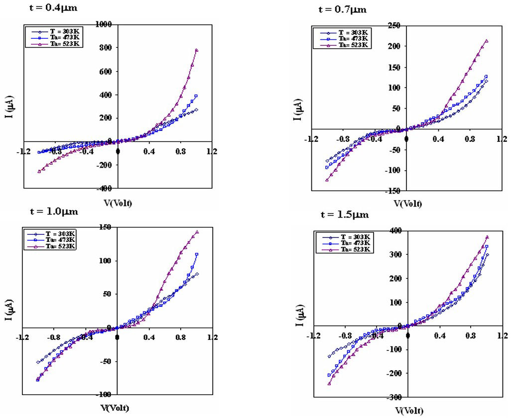
In the present work we are reporting the preparation conditions of GaAs thin films and the technique which was employed to produce films deposited on Ge wafers substrate at constant substrate temperature by thermal evaporation method are described. Also it includes photovoltaic measurements which are presented by current – voltage characteristics, photocurrent, short – circuit, open – circuit voltage of GaAs/Ge heterojunction, at room temperature and different annealing temperatures have been measured. All the samples were prepared under constant conditions (pressure, substrate temperature and rate of deposition); the main parameters that control the nature of the film properties are thickness (0.4, 0.7, 1.0 and 1.5) μm and annealing temperature (473 and 523) K. The dark current decreases with increasing of thickness; whereas increases slightly with increasing of annealing temperatures. Under illumination, the photocurrent increases with increasing of annealing temperatures and decreases with increasing of thickness except at thickness equal to 1.5m. There is a linear increasing in the first part of the relation between Isc and Voc with incident power intensity and then the saturation region appeared. The Isc and Voc decrease with increasing of thickness, while increase with increase of annealing temperatures.
Downloads
References
Y. H. Hu, M. J. Li, Y. P. Zhou, H. Xi, and T. C. Hung, Multi-physics investigation of a GaAs solar cell based PV-TE hybrid system with a nanostructured front surface, Sol. Energy 224 (2021) 102-111 DOI: https://doi.org/10.1016/j.solener.2021.06.003
T. Y. Sabri, S. K. Jasim, A. A. Habeeb, and A. S. Jasim, Preparation and study Ag nanoparticles via PLAL technique: Influence of different number of pulses, Int. J. Nanoelectron. Mater. 17 (2024) 45-51 DOI: https://doi.org/10.58915/ijneam.v17i1.458
C. Wang, Z. Zhang, X. Jing, Z. Yang, and W. Xu, Optimization of multistage femtosecond laser drilling process using machine learning coupled with molecular dynamics, Opt. Laser Technol. 156 (2022) 108442 DOI: https://doi.org/10.1016/j.optlastec.2022.108442
E. S. Goh, T. P. Chen, C. Q. Sun, and Y. C. Liu, Thickness effect on the band gap and optical properties of germanium thin films, J. Appl. Phys. 107 (2010) 023506 DOI: https://doi.org/10.1063/1.3291103
C. Han et al., Microstructure evolution and ductility improvement of additively manufactured biodegradable zincmagnesium alloys via annealing, Int. J. Bioprint. 10 (2024) 3034 DOI: https://doi.org/10.36922/ijb.3034
J. Peng et al., Numerical simulation and process parameter optimization of laser spot welding for ultra-thin sheets, Opt. Laser Technol. 193 (2026) 114240 DOI: https://doi.org/10.1016/j.optlastec.2025.114240
S. K. Jasim, A. M. Shano, and S. K. Adnan, Zinc oxide poly crystals heterojunction and infrared-blind UV-photodetector, J. Nano-Electron. Phys. 16 (2024) 01012 DOI: https://doi.org/10.21272/jnep.16(1).01012
Y. Zhang, Z. Zhang, X. Zhang, K. Wu, R. Riedel, D. Hu, and J. Sun, Machine learning guided design and ablation behavior of ZrC-TaC-SiC ternary coatings, Corros. Sci. 260 (2026) 113499 DOI: https://doi.org/10.1016/j.corsci.2025.113499
S. K. Jasim, S. M. A. Al Hussan, and M. T. Abd, Improving the mechanical properties of dental fillings by adding TiO2 NPs prepared laser ablation, BioNanoScience 15 (2025) 330 DOI: https://doi.org/10.1007/s12668-025-01970-y
R. Kumar et al., Realization of high-quality InGaAs/GaAs quantum dot growth on Ge substrate and improvement of optical property through ex-situ ion implantation, J. Lumin. 223 (2020) 117208 DOI: https://doi.org/10.1016/j.jlumin.2020.117208
Y. Jiang, H. Shen, T. Pu, C. Zheng, Q. Tang, K. Gao, and Y. Liu, High efficiency multi-crystalline silicon solar cell with inverted pyramid nanostructure, Sol. Energy 142 (2017) 91-96 DOI: https://doi.org/10.1016/j.solener.2016.12.007
I. Hilmi, M. K. Adam, J. Purwadi, Q. M. B. Soesanto, and D. Y. Kusuma, Influence of annealing on the physical and optical properties of Ge thin films deposited using thermal evaporation, J. Phys. Appl. 7 (2025) 28-32
A. H. Ahmed, A. S. Jasima, and S. K. Jasim, Synthesis of gold nanoparticles by pulsed laser ablation and its study physical and mechanical properties, Int. J. Nanoelectron. Mater. 17 (2024) 634-644 DOI: https://doi.org/10.58915/ijneam.v17i4.1465
I. Demir, A. E. Kasapoǧlu, H. F. Budak, E. Gür, and S. Elagoz, Influences of thickness and temperature of low temperature GaAs buffer layer on two-step MOVPE grown GaAs/Ge heterostructures, Eur. Phys. J. Appl. Phys. 90 (2020) 20301 DOI: https://doi.org/10.1051/epjap/2020190216
W. Kou, J. Gou, J. Gao, J. Zhu, Z. Li, and J. Wang, Effects of arc oscillation on interface behavior and properties of additivemanufactured 2319/5356 dissimilar aluminum alloy, Mater. Today Commun. 47 (2025) 113068 DOI: https://doi.org/10.1016/j.mtcomm.2025.113068
S. K. Jasim, S. M. A. A. Hussan, A. S. Noori, and A. A. Habeb, Determine surface plasmon resonance and effect parameters laser ablation on Cu and Zn nanoparticles, AIP Conf. Proc. 3219 (2024) 060008 DOI: https://doi.org/10.1063/5.0236469
Y. Zhou, W. Liu, S. Zhang, H. Liu, Z. Wu, and X. Wang, Ecofriendly flame-retardant phase-change composite films based on polyphosphazene/phosphorene hybrid foam and paraffin wax for light/heat-dual-actuated shape memory, ACS Appl. Mater. Interfaces 16 (2024) 7754-7767 DOI: https://doi.org/10.1021/acsami.3c16953
J. Zhou et al., GaAs/GeSn/Ge n-i-p diodes and light emitting diodes formed via grafting, J. Vac. Sci. Technol. B 42 (2024) DOI: https://doi.org/10.1116/6.0003619
E. Erofeev and V. Kagadei, Formation of Ge/Cu ohmic contacts to n-GaAs with atomic hydrogen pre-annealing step, Proc. SPIE 7521 (2010) 176-181 DOI: https://doi.org/10.1117/12.853639
I. Kabacelik, M. Kulakci, and R. Turan, Structural and electrical analysis of poly-Ge films fabricated by e-beam evaporation for optoelectronic applications, Mater. Sci. Semicond. Process. 56 (2016) 368-372 DOI: https://doi.org/10.1016/j.mssp.2016.09.023
N. A. Pakhanov and M. Z. Shvarts, Designing of lightweight and ultrathin III-V/Ge solar cells for flexible space and terrestrial photovoltaic blankets, Phys. Status Solidi A 221 (2024) 2300709 DOI: https://doi.org/10.1002/pssa.202300709
R. Naik, A. Aparimita, D. Alagarasan, S. Varadharajaperumal, and R. Ganesan, Linear and nonlinear optical properties change in Ag/GeS heterostructure thin films by thermal annealing and laser irradiation, Opt. Quantum Electron. 52 (2020) 136 DOI: https://doi.org/10.1007/s11082-020-2245-6
X. Zhang, J. Sun, Y. Zhang et al., Machine learning for phase prediction of high entropy carbide ceramics from imbalanced data, npj Comput. Mater. (2026) DOI: https://doi.org/10.1038/s41524-025-01873-2
G. Cai, Y. Huang, Y. Qing, and R. D. K. Misra, Investigation of microstructure and texture evolution of nickel-saving duplex stainless steels containing Y, J. Mater. Res. Technol. (2026) DOI: https://doi.org/10.2139/ssrn.5974916
Z. Zhang et al., Synergistic radiation effect of 300 MeV proton and heavy ion on electrical characteristics of β-Ga2O3 SBD, IEEE Trans. Nucl. Sci. (2026)
Y. Liu et al., Effect of annealing temperature on microstructure and properties of stainless steel/copper composite strips, Adv. Compos. Hybrid Mater. 9 (2026) 103 DOI: https://doi.org/10.1007/s42114-026-01648-3
Downloads
Published
How to Cite
Issue
Section
License
Copyright (c) 2026 Imad N. Kashkool, Saif Khalel Jasim, Aws K. Mohammed, Mohamed T. Abd; Ahmed M. Shano

This work is licensed under a Creative Commons Attribution-NonCommercial-NoDerivatives 4.0 International License.
Authors retain copyright and grant the Revista Mexicana de Física right of first publication with the work simultaneously licensed under a CC BY-NC-ND 4.0 that allows others to share the work with an acknowledgement of the work's authorship and initial publication in this journal.